Ian Smythe, VP Product Marketing and Strategic Alliances

Key Themes from the Summit
Joint solution reduces risk and accelerates time-to-silicon for advanced semiconductor platforms
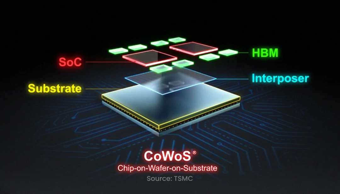
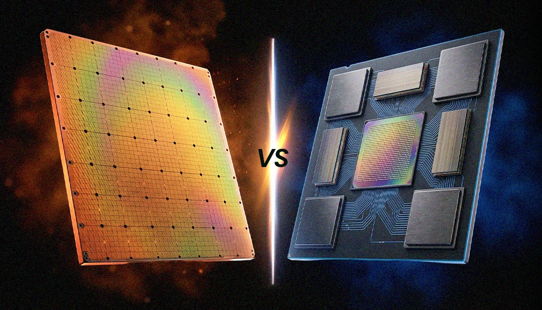
The tone was clear across sessions and keynotes: AI is driving unprecedented compute demand, and infrastructure must scale in new ways to support it.
Where Baya Fits
In this context, the conversations at the Baya booth took on even greater importance. With demonstrations of our software-driven, scalable data movement solutions, we showed how Baya is addressing one of the most pressing challenges in AI infrastructure: moving data efficiently at massive scale. Our fabric IP and tools are designed to give system architects the flexibility to explore new architectures, optimize compute efficiency, and reduce bottlenecks that otherwise limit system performance.
What resonated most with visitors was how seamlessly our approach can be integrated into diverse design flows, whether for AI accelerators, cloud and data center platforms, or edge applications, making Baya not just a niche solution, but a foundational enabler for the future of compute. The deep technical and commercial discussions we had confirmed that data movement has become a first-class design concern, and that Baya is well-positioned to help customers and partners navigate this transition.
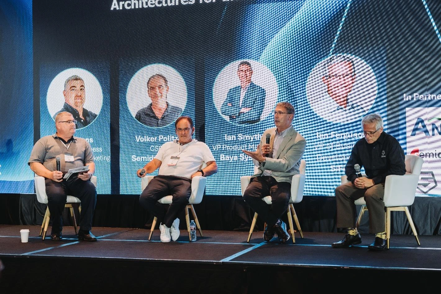
The summit also provided opportunities for Baya to share its perspective more broadly. I had the privilege to speak on the panel RISC V: Alternative Architectures for Efficient System Scaling, highlighting how open standards and chiplet ecosystems are shaping future architectures, and our team also spoke at the Synopsys AI Chip Design Startup Forum, where we shared insights on what it takes to build and scale an AI startup from the first idea through tape-out and beyond. This discussion resonated strongly with the audience, offering practical lessons, candid perspectives, and inspiration for entrepreneurs and innovators navigating the complex journey of bringing advanced semiconductor and AI solutions to market.
Look out for the recordings of these panels, which will be available soon.
What a week!
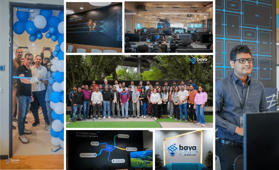
On a personal note, it was the perfect way to begin my journey with Baya. I’m delighted to have joined as VP of Product Marketing, and I’ve been deeply impressed by the impact Baya already has in the ecosystem. Meeting our customers last week only reinforced my excitement about the opportunities ahead, and it was equally inspiring to spend time with the amazing Baya team, a group of experts driving scalable data movement solutions into the heart of AI infrastructure.
The AI Infra Summit showed the scale of the challenge and the ambition of the solutions. At Baya, we’re excited to play a defining role in this journey.
What a week one, and it’s just the beginning!
About Baya Systems
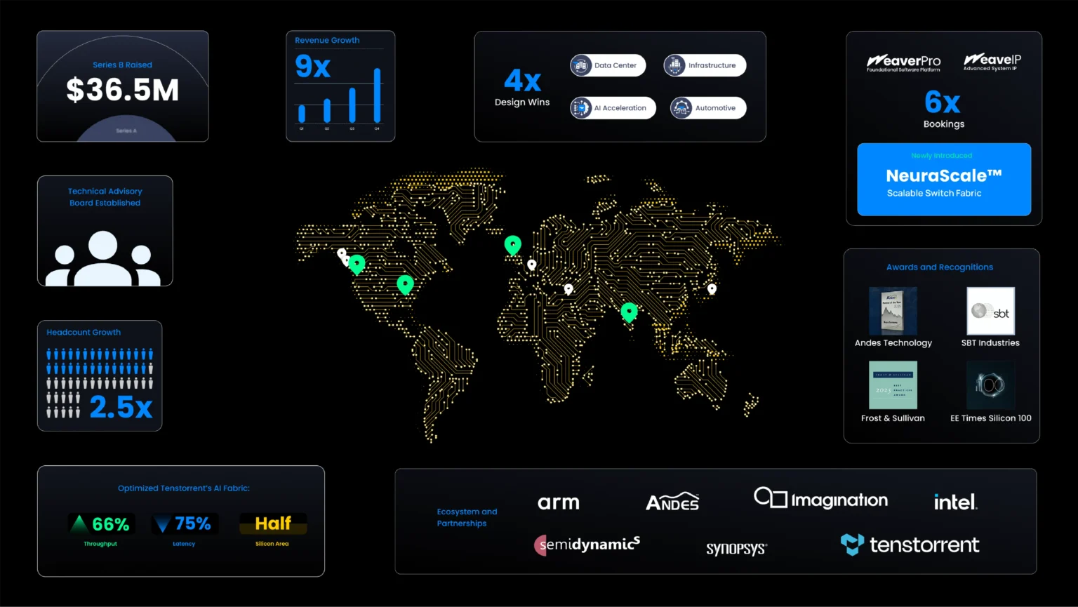
Baya Systems is leading the next wave of foundational, high-performance, and modular semiconductor systems technologies that are chiplet-ready and accelerate intelligent compute everywhere. Inspired by the baya bird’s nest-weaving ability, Baya integrates best-in-class compute, communication, and I/O components into seamless, energy-efficient solutions. Its software-based design and exploration platform enhances performance, yield and reusability, enabling cutting-edge, cost-effective innovation across multiple industries. A member of the EE Times 2025 Silicon 100 and recipient of Frost & Sullivan’s 2025 Technology Innovation Leader award in semiconductor IP interconnect, and winner of the 2025 EPDT Product of the Year Award, Baya is ISO 9001:2015 certified and backed by leading investors including Matrix Partners, Maverick Silicon, Synopsys Inc., and Intel Capital. For more information, visit https://bayasystems.com or follow us on LinkedIn.
Share this article
Share this article