These are eye-popping numbers, both in terms of monetary value and compute power. Looking at OpenAI’s situation, however, the massive spend is justified: they’re now supporting 800 million active users weekly, and they need the infrastructure to support those users and further runaway growth.
OpenAI’s move also illustrates the prevailing trend for current tech investment, which is a heavy focus on AI development and the datacenter infrastructure to support it. But what is hidden in this noise is how OpenAI and others are planning to address looming needs for more specialized capabilities and customized systems that deliver not just the performance, but that optimize the return on investment.
Fundamentally, the latency wall continues to be a challenge, and leaders like Nvidia have been prescient and proactive in addressing these challenges—first with the launch of their NVLink for scale-up, and then with the purchase of Mellanox systems, which became the backbone of scale-out infrastructure while also bringing crossbar and switching expertise, such as the SHARP (Scalable Hierarchical Aggregation and Reduction Protocol) that added to NVSwitch’s lead. They most recently added to this arsenal with the acquisition of Enfabrica, another emerging player that promises an elastic AI Memory Fabric System. This has been the foundation of Nvidia’s runaway success in Data center scale-up and scale-out.
The real question is this: has the semiconductor industry taken the time to invest in building a proper support ecosystem for this purpose now? i.e. focus on balancing raw compute power with other addressing the real challenges around data movement latency, energy consumption, and even the physical footprint of a system.
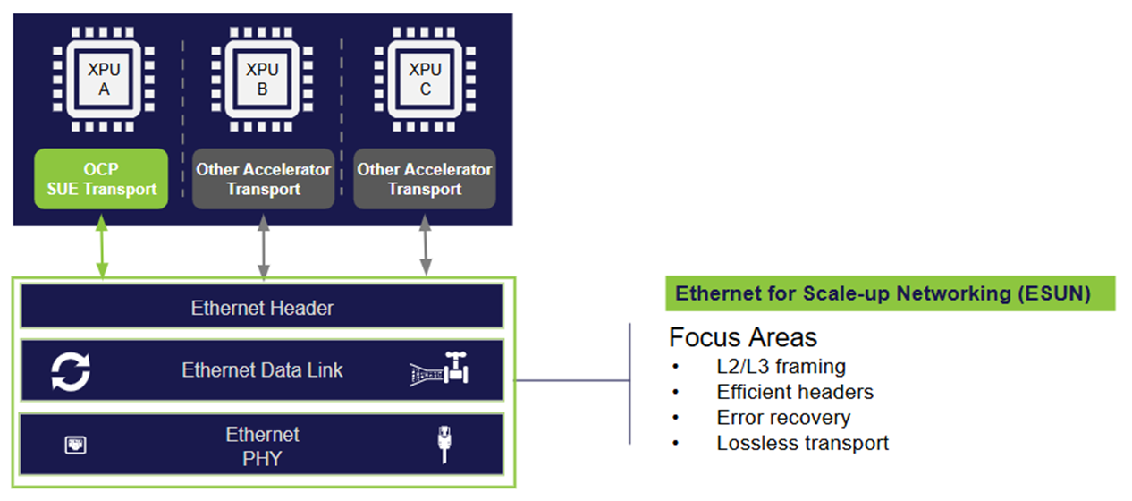
Clearly, the industry did identify the challenges around data movement for training and, to a lesser extent, inference, and responded by investing in multiple standards. The first investment is a consortium that includes hyperscalers, datacenter and networking infrastructure heavyweights including Alibaba, AWS, Google, Meta, AMD, Intel, Broadcom and Cisco around Universal Accelerator Link (UALink) that is tailor-made for Scale-Up and will be seeing products launched shortly. The OCP Consortium led by switching giants like Broadcom is leaning on the ubiquity of the Ethernet standard by championing ESUN (Ethernet for Scale-Up Networking). Both highlight the clear focus on data movement and transfer speed, which arise from highly complex and scalable systems of processors that are needed for growing AI model size. UltraEthernet consortium (UEC) has also been building momentum for scale-out.
Now the question is: can the rest of the semiconductor industry accelerate the ecosystem that supports these standards? Or, rapidly drive to resolve the path to establishing the preferred standard? Will this help balance raw compute power with improved efficiency in data movement latency and lower energy consumption per token or per inference?
Does this immediately address the energy consumption challenge which is becoming a major concern? For example, even as OpenAI continues to make big announcements, the datacenters fueling its growth have driven up wholesale electricity prices by as much as 267% so far, and the IEA expects that datacenters’ energy demands will more than double (to 945 terawatt-hours) by 2030—the more energy datacenters consume, the more prices are driven up, assuming that companies make no changes.
No, the energy consumption challenge is not immediately addressed by simply establishing a preferred standard. However, by accelerating an open ecosystem that supports highly efficient data-movement for both scale-up and scale-out, the industry can, and must, re-orient toward a customer-focused, optimized design and deployment strategy that allows for fit-for-purpose, highly scalable, customized solutions—not just heavyweight GPU-based systems for ever-evolving workloads and demands. It’s not just good for the semiconductor industry; it’s good for the bottom lines of datacenters and AI companies, and more importantly, sustainability for the planet.
In just one example, fabric channels in high-performance silicon can take up to 15-30%1 of the system’s overall power consumption and die area. With Tenstorrent, Baya Systems has already shown that modern fabric solutions such as Baya Systems’ WeaveIP™ portfolio can not only reduce power consumption and increase performance with more efficient data movement but also achieve the same functionality in half the silicon area, while reducing latency by up to 75%. More importantly, the Baya’s WeaverPro™ FabricStudio data-driven design platform enabled rapid re-architecture with advanced performance analysis, and workload simulation, in a matter of weeks.
Similarly, Baya’s NeuraScale product, which radically simplifies crossbar switching for scale-up and scale-out networking for the standards mentioned above, can significantly reduce the development time, silicon footprint and scalability of switching solutions through chiplets, boosting energy efficiency and reducing (picoJoules) pJ/inference while maintaining the key benefits of the crossbar behavior. This is fundamental to the next round of AI scaling.
The broader impact from investment into systems development for the future, however, needs to go beyond energy savings. The ability to optimize routing post-silicon to adapt to future workloads helps future-proof systems. Future-proofed chips and chiplets designed to adapt to changing workload demands are a much-better long-term investment that will reduce development and maintenance costs. With fewer chips needed to get the same or better performance, substantially increasing the compute density in data centers could result in fewer new data centers being built, further driving down energy costs as well as land, construction, and maintenance costs. These benefits all compound on each other and free up capital for more R&D or other long-term investments.
It’s tempting for the industry to continue its current course—OpenAI’s partnerships make it clear the demand is there, but the investment v/s return doesn’t seem sustainable at this pace. So, the transition to chiplet-integrated, optimized, scalable system solutions is necessary to provide sustainable growth, faster innovation, and the profitable proliferation of AI.
Meet the future of semiconductor IP today: contact us to learn more.
1Technical Report No. UCB/EECS-2023-168
http://www2.eecs.berkeley.edu/Pubs/TechRpts/2023/EECS-2023-168.html