Standard die attachment techniques fail entirely at this size due to thermal mismatch, so Cerebras developed a custom connector and a layered clamping assembly that holds the wafer mechanically against the PCB and heat exchanger, absorbing displacement without breaking a single electrical contact.
Even the relationship between compute and memory was reinvented. Weight streaming disaggregates parameter storage from the processor entirely, allowing models far larger than available on-chip memory to run without performance penalty, making a fundamental constraint into just another design variable.
Any of these innovations would be a significant breakthrough on their own. Together, they underwrite Cerebras’ central architectural innovation: SwarmX, a 2D mesh fabric that spans the entire wafer surface and lets any core communicate with any other without ever leaving the silicon.
No hop to a neighboring chip. No NVLink traversal. No off-package round trip. Just data, moving at the speed of the substrate.
The real challenge that the next generation of AI infrastructure must overcome is how fast and efficient data moves, not just how fast each compute engine executes. On the SoC and chiplet level, recognition of this problem is what led to on-die fabrics and high-bandwidth memory. Without the fast data movement they enable, compute starves.
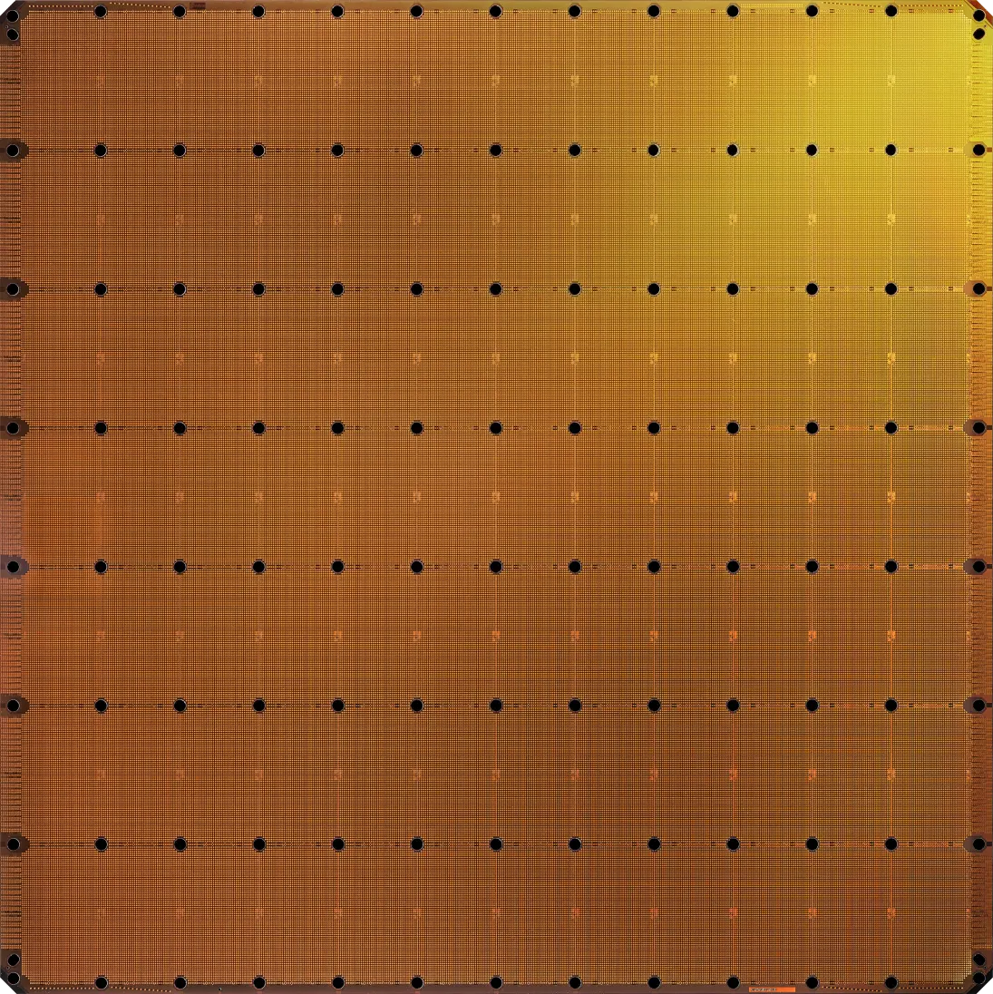
SwarmX extends that principle to an entirely new scale: the wafer. Data can now move without penalty over a surface of 46,000 square millimeters of unified silicon on the WSE-3. To put it in perspective, that is over 60x the size of an Nvidia Blackwell die. The performance implications scale accordingly.
We’re at the point where Cerebras’ local solution becomes an industry-wide question. If moving data at substrate speed across a wafer changes what AI compute can do, what does it mean for every other architecture still paying the inter-chip tax?
Part 2 Coming Soon: Two Paths, One Wall. How the rest of the industry is chasing the same constraint from the opposite direction.