Scale-within, Scale-up and Scale-out Fabrics Enable Efficient AI Acceleration
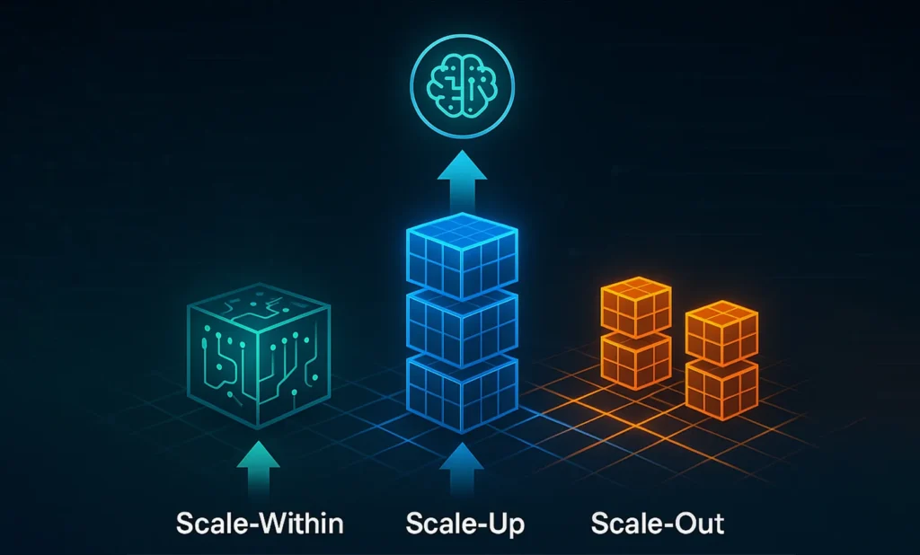
Home / Scale-within, Scale-up and Scale-out Fabrics Enable Efficient AI Acceleration While GPU performance has been the focus in data centers over the last few years, the performance of fabrics has become a key enabler or bottleneck in achieving the throughput and latency required to create and deliver artificial intelligence at scale. Read More Latest […]
Baya Systems to Share Insights on Chiplet Integration, AI Scalability at DAC 2025

Home / Baya Systems to Share Insights on Chiplet Integration, AI Scalability at DAC 2025 SAN JOSE, Calif., June 16, 2025 /PRNewswire/ —Baya Systems, a leader in high-performance semiconductor system technologies, will join industry innovators at the 2025 Design Automation Conference (DAC) to showcase advances in chiplet-ready design and system scalability for the next generation of AI. Read More Latest […]
Why Your Heterogeneous Compute System Isn’t Performing… and What to Do About It
Home / Why Your Heterogeneous Compute System Isn’t Performing? and What to Do About It ? Are you designing multi-core or hybrid CPU/GPU systems, but still not hitting your performance targets? You’re not alone. As system architects strive to build ever more powerful SoCs, the focus is too often on compute abundance. Read More Latest […]
That Tech Pod: The Data Movement Crisis in AI – How Baya is Rethinking AI Infrastructure
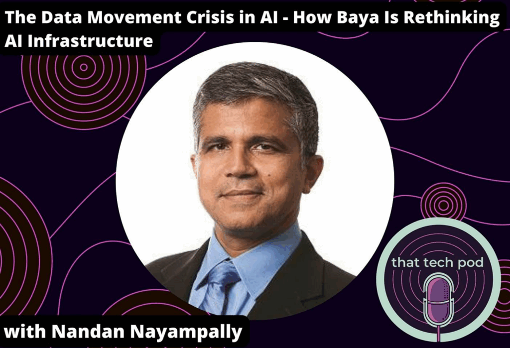
Home / That Tech Pod: The Data Movement Crisis in AI – How Baya is Rethinking AI Infrastructure Laura Milstein and Kevin Albert sit down with Nandan Nayampally, the Chief Commercial Officer at Baya, to discuss the shifting landscape of intelligent computing and the hidden challenges behind AI innovation. Listen Here Latest News Baya Systems […]
Embedded world 2025 – Baya Systems Intro with Nandan Nayampally

Home / Embedded World 2025 – Baya Systems Intro with Nandan Nayampally Join Nandan Nayampally at Embedded World 2025 as he introduces Baya Systems and our vision for driving innovation in AI, HPC, and semiconductor architectures. Watch the full video to see how we’re shaping the future of intelligent computing. Watch here Latest News Baya […]
Baya Systems AI-optimized chiplet interconnects at Embedded World 2025 WeaverPro, WeaveIP RISC-V HPC

Home / Baya Systems AI-optimized chiplet interconnects at Embedded World 2025 WeaverPro, WeaveIP RISC-V HPC At Embedded World 2025, Baya Systems showcased its approach to solving one of the biggest challenges in high-performance computing—efficient data movement. Nandan Nayampally, the company’s Chief Commercial Officer, explained how Baya is addressing bottlenecks in intelligent compute acceleration by focusing […]
Baya Systems New NeuraScale Upscales Traditional Switching Architectures
Home / Baya Systems New NeuraScale Upscales Traditional Switching Architectures In order to address the significant scaling and data movement challenges in AI infrastructure that are propelling advanced SoCs and innovative 3D chiplet-based designs, Baya Systems unveiled its new NeuraScale switch fabric technology. Read more Latest News Baya Systems Receives Frost & Sullivan’s 2025 Award […]
Baya’s NeuraScale Fabric Sees 100x AI Chiplet Boost
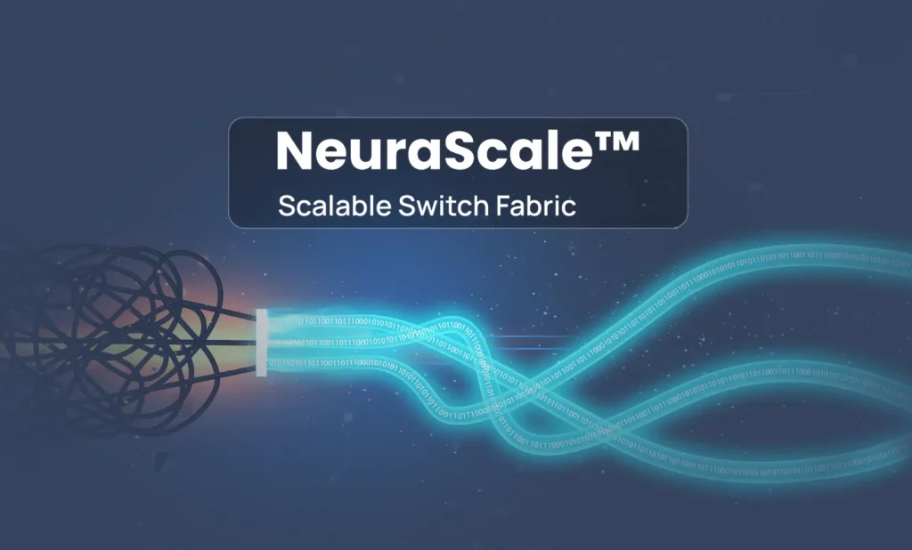
Home / Baya’s NeuraScale fabric sees 100x AI chiplet boost The NeuraScale switch fabric technology is designed to overcome critical scaling and data movement challenges in AI infrastructure with a 100x increase in node density for the UALink standard. This is a key factor for AI workloads that need higher performance, throughput and efficiency where […]
EDA Cafe: Solving AI’s Biggest Challenge

Home / EDA Cafe: Solving AI’s Biggest Challenge via EDA Cafe: As AI scales, data movement and connectivity have become the biggest challenges. Baya Systems is addressing this with IP subsystems that optimize high-performance, scalable AI systems. In a recent EDA Cafe interview, CEO Sailesh Kumar discusses how Baya’s software-driven interconnect solutions are enabling efficient, […]
citybiz: Q&A with Nandan Nayampally, CCO of Baya Systems

Home / citybiz: Q&A with Nandan Nayampally, CCO of Baya Systems via citybiz: In a new citybiz Q&A, Nandan Nayampally, CCO of Baya Systems, discusses how AI, HPC, and automotive industries are driving the need for scalable, high-performance interconnect solutions. He shares insights on WeaverPro and WeaveIP, Baya’s Series B funding, and how a software-driven approach is […]